


Spreading inductance in wide cavities1 Iulie 2020
Introduction
In this article I direct my attention toward the study of inductance. The reason why this measure is important to be studied is the same as previously mentioned with regard to capacitance, which I have in depth investigated in a previous article: almost every interconnect can be characterized up to a certain frequency as a lumped RLCG circuit. This is also the case of parallel planes so ubiquitously spread in the power integrity field which can also be characterized as a series (or parallel) LC circuit, where the C stands for parallel plate capacitance and the L for inductance.
If capacitance is a simple and straightforward property which can easily be approximated using the parallel plate formula as I have previously done in this article, inductance is the rogue one from the LC pair. A simple approximation for inductance homologous to the one for capacitance also exist but it assumes a uniform current distribution into the cavity. Unfortunately, current density tends to be uniform only in narrow conductors while spreading in different ways to follow the path of minimum impedance at high frequencies in wide cavities.
In this article I investigate the inductance associated with wide cavities using ANSYS HFSS 3D electromagnetic simulator and I also discuss how this property influences the impedance profile of such a structure. The non uniform path that a current follows at high frequencies can only be correctly investigated using a full-wave field solver. The existing analytical approximations in the literature are also presented here along with their limitations. Results from these formulas are also compared to the ones obtained from ANSYS HFSS.
Materials and Methods
In the case of a conductor modeled in the shape of a closed loop crossed by a current we can extract the loop inductance with the equality from Equation 1 where Ψloop is the total number of magnetic flux lines passing through the closed loop and I is the current crossing the conductor. Subsequently, the total number of magnetic field lines can be obtained by integrating over the whole surface B, the magnetic field density.
 Equation 1: Inductance definition formula
The formula from Equation 1 is often difficult to understand, almost never solved by hand and only used in numerical algorithms. Eric Bogatin best describes inductance in [1] in a much easier and understandable way: "Just as capacitance is a measure of the efficiency of two conductors for storing charge at the price of voltage, inductance is a measure of the efficiency of a conductor loop in storing magnetic field lines at the cost of current in the loop". Moreover, he also enumerates the complex mathematical principles that stand behind the concept of inductance simplified in a few essential observations:
- magnetic field rings appear only as closed rings
- any current passing a conductor generates magnetic field rings closing around that conductor
- magnetic field lines do not interact with dielectric materials
- the number of magnetic field lines surrounding a conductor is proportional to the current through the conductor
- if the number of magnetic field lines around a conductor changes, a voltage will be generated across that conductor
- energy is stored in the magnetic field lines, the higher the number of field lines, the more energy being stored
In the incipient part of a design, simple analytical approximations are needed to estimate properties such as inductance. The kind of approximations such as the parallel plate capacitance should not be used for signing off a design. Exact expression that can accurately calculate a figure of interest are preferred if possible. Unfortunately, in the case of loop inductance we can only develop this kind of expression for three specific geometries: coaxial cable, two round rods and a rod over a plane, none of which is close to parallel planes. For any other structure the loop inductance can only be exactly calculated if the fundamental definition is used.
Homologous to the parallel plate capacitance, an analytical approximation also exist for the loop inductance of two parallel conductors separated by a dielectric. This is the expression from Equation 2, where μ0 is the permeability of free space equal with 4 · π · 10 -7 H/m and Len, w, h are the length, width and height of the structure. The product μ0 · h is named Lsquare and is the sheet inductance, how much inductance resides in a square from a specified geometry.
 Equation 2: Loop inductance for narrow long cavities
As the parallel plate capacitance formula has its limitations due to fringing effect investigated in this previous article, so does the expression from Equation 2. This one is only accurate for narrow and long conductors, where the current distribution is constant in the whole surface. With other words, only geometries with aspect ratios w/h higher than 10 will lead to accurate results. For lower aspect ratios, transmission line approximations for inductance should be used [2].
Equation 2 also gives us the three general design principles to reduce loop inductance: lowering the length of the parallel conductors, making the conductors wider and bringing them closer together. This is the reason why wide, closely spaced parallel planes are used in power distribution networks in high speed circuit boards. Even if large power planes also bring a higher parallel plate capacity, the low loop inductance that these large power plane bring is by far a higher contribution than their capacitance in the design of a PDN.
Using Equation 2 to quickly investigate a simple narrow cavity of 80 MILs width, height of 7.87 MILs and a length of 80 mm provided a result of 9.88 nH for the loop inductance. Using also ANSYS HFSS to extract this inductance I obtain a value of 8.34 nH, close to the initial estimate. Differences between analytical and simulation values were caused by using Equation 2 at the margin of its applicability domain, for a structure with w/h 10. For the same geometry I also performed a transient simulation by launching a 35 ns rise time signal from a 5 MILs contact point situated at one end and saving the current density in the upper plane. Observe in Figure 1 how the current spreads almost immediately into the narrow plane. However, the few ps it takes the current to spread into the full width of the structure contribute to a small non uniform density.
 Figure 1: Current density in the upper plane of an 80 MILs narrow cavity with a 7.87 MILs
separation between planes (w/h ≈ 10) when a 35ns rise time wave is launched from one end
from a 5 MILs width contact point. Observe how the current almost immediately spreads
into the whole width of the narrow plane.
Figure 1: Current density in the upper plane of an 80 MILs narrow cavity with a 7.87 MILs
separation between planes (w/h ≈ 10) when a 35ns rise time wave is launched from one end
from a 5 MILs width contact point. Observe how the current almost immediately spreads
into the whole width of the narrow plane.When the cavity is not long and narrow but wide, the current density in the copper planes is by far uniform. When a signal in launched from the contact point into a cavity it spreads radially until it hits the walls of that cavity, gets reflected and fades out in the end. At different points into the cavity the current density differs, being higher near the contact point and lower towards the margin of the cavity, leading to an inductance highly dependent of port location. The loop inductance when the current spreads outward from a small contact region is therefore refereed as the spreading inductance. Equation 3 is an analytical expression for the spreading inductance of a cavity provided in [1] by solving the definition from Equation 1.
 Equation 3: Spreading inductance in circular cavities
Equation 3 is only accurate for a circular cavity with the diameter Dcavity probed from a central contact point with a diameter DVIA. The cavity is formed by two parallel planes separated by a dielectric of height h. This geometrical limitation of a circular shape is a result of integrating the original definition of inductance over a circular area [1]. However, it gives an insight into the control knobs we have for lowering the spreading inductance: shorter cavities and as closed as possible planes. Once again, notice how important is to have the planes spaced as close as possible in power distribution networks.
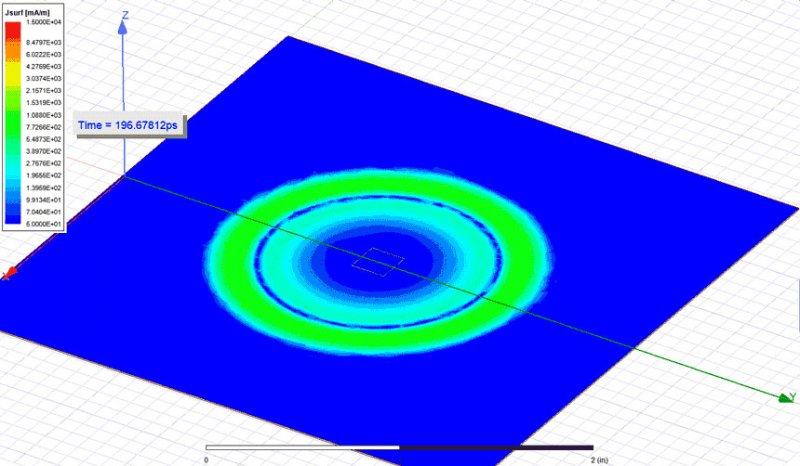
As previously mentioned, spreading inductance is all about the the current distribution in the planes when wide cavities are subjected to analysis. In order to better present the concept of current density in wide planes I performed three transient simulations for a 80 mm square structure with the planes separated by 7.87 MILs of dielectric material. I launched a 35 ns rise time signal from the center, edge and corner of this structure through a 20 MILs contact point and investigated the first 200 ps of current propagation through the structure. The results are displayed in Figures 2, 3 and 4. Observe in these three cases how the current spreads from the source as the ripples of water in a pond in four quadrants. When we restrict the area at only two quadrants as is the case of the margin contact point from Figure 3, a higher current density will appear leading to roughly twice as much spreading inductance (the exact numbers are presented in the Dissemination and Results section). The same premises applies when the contact point is situated in the corner, leading a four times higher inductance due to the current spreading in only one quadrant.
 Figure 2: Current density in the upper plane of an 80 mm square cavity with a 7.87 MILs
separation between planes when a 35ns rise time wave is launched from a 20 MILs width
contact point situated in the center. Observe how the current spreads 360° around the source
point.
Figure 2: Current density in the upper plane of an 80 mm square cavity with a 7.87 MILs
separation between planes when a 35ns rise time wave is launched from a 20 MILs width
contact point situated in the center. Observe how the current spreads 360° around the source
point. Figure 3: Current density in the upper plane of an 80 mm square cavity with a 7.87 MILs
separation between planes when a 35ns rise time wave is launched from a 20 MILs width
contact point situated on one edge. Observe how the current can only spread 180° around the
source point.
Figure 3: Current density in the upper plane of an 80 mm square cavity with a 7.87 MILs
separation between planes when a 35ns rise time wave is launched from a 20 MILs width
contact point situated on one edge. Observe how the current can only spread 180° around the
source point. Figure 4: Current density in the upper plane of an 80 mm square cavity with a 7.87 MILs
separation between planes when a 35ns rise time wave is launched from a 20 MILs width
contact point situated on a corner. Observe how the current can only spread 90° around the
source point.
Figure 4: Current density in the upper plane of an 80 mm square cavity with a 7.87 MILs
separation between planes when a 35ns rise time wave is launched from a 20 MILs width
contact point situated on a corner. Observe how the current can only spread 90° around the
source point.The impedance profile of a cavity reveals tons of information regarding geometric aspects and not only. Suppose we probe the same 80 mm square cavity from a contact point located in its center, with no other shorting wall applied to its margins, what would be the expected result? The impedance profile of the cavity will have three intervals, the first starting at low frequencies dominated by the capacitance of the planes, Ccavity, the second dominated by the spreading inductance, Lspread and the third where modal resonances take place in the high frequency domain.
Focusing for now on the first two interval, we can easily approximate the cavity as a lumped series LC circuit (or parallel if we were to short its edges with an perfect conductor wall). The point separating the capacitive from the inductive behavior is nothing more than the self-resonant frequency (abbreviated SRF) of a series LC circuit which can be calculated using Equation 4.
 Equation 4: Self resonant frequency forumula
The capacitance of the cavity is independent of the probing location and can be accurately calculated if the fringing effect is taken into account as discussed in this previews article. However, the spreading inductance that in some cases can be calculated using Equation 3 is highly influenced by the probing location. Subsequently, the SRF point will have different values for different probing locations.
So far I have only discussed about the spreading inductance as seen from a contact point placed in different locations of a structure looking into the cavity with the current traveling radially outwards from that contact point. This is roughly the minimum series inductance the current sees as it travels the cavity. Any other configuration will only increase its inductance. Take for example a more practical case, the spreading inductance between two contact points from the terminal of a SMD capacitor to the pad of a BGA. There are now two contact points involved, the VIA below the BGA pin and the one next to or in the pad of the capacitor. These two contact points lead to a higher density current which subsequently leads to an increased spreading inductance.
A simple approximation for the spreading inductance from one point to another is provided by Equation 5 [1]. This formula was developed based on the following premises: the first contact point with a diameter d known is considered to be in the center of a circle and the second one is placed on the margin of that imaginary circle. If the spacing of the two points named s here is known, the diameter of the circle is also known as 2·s. The spreading inductance from the center of this imaginary cavity would have the expression previously presented in Equation 3 if only one point was involved but due to the current concentration towards the second contact point, the result must be scaled with a certain scaling factor, found in this analysis to be equal with 2.5. The final formula is provided in Equation 5.
 Equation 5: Point to point inductance formula
Considering the premises that led to Equation 5, its limitations are quite clear: when the spacing between the points becomes comparable to one length of the cavity, the spreading inductance will in reality be larger than the one predicted by the analytical formula. This is easily explained in this case since when one contact point of both are close to the margins of the cavity, current crowding is no longer only caused by the two contact points but also by the margin of the planes.
Equation 5 also gives insight about how the spreading inductance can be reduced with by far the highest positive impact coming from lowering the spacing between planes. Bringing the two contact points closer also has an impact but not as much as lowering the spacing between planes. The interesting observation is that the contact point diameter has the same influence as the distance between the two points: they both slowly influence the spreading inductance with a small logarithmic dependency. This is also the main reason why multiple VIA whole when connecting a capacitor to the power planes significantly reduce inductance.
Simulation setup
In this article I was interested to investigate spreading inductance and what limitations do the analytical formulas presented in the previous section have. Using a spreadsheet I implemented these formulas for different structures and compared analytical results with the ones simulated in ANSYS HFSS. I created three parallel plane structures for this study, two squares with the length of 80 mm and a circle with the diameter of also 80 mm. The dielectric between copper planes was a classic FR4 with height of 0.1, 0.2 and 0.565 mm depending of the study performed. Port size also has an important influence as previously mentioned and since I also wanted to investigate this variation I used different port sizes of 5, 10 and 20 MILs.
Displayed in Figure 5 is the round structure I used to investigate the spreading inductance when the cavity is probed from center. Only one lumped port was added in the middle of this cavity and the impedance profile from 10 MHz to 1 GHz was simulated. Variations of 0.1, 0.2 and 0.565mm for height and of 5, 10 and 20 MILs for port width (what would be taken as DVIA in Equation 3) were investigated. The impedance profile was expected to look like the one of a series LC circuit, capacitive at low frequencies and inductive above the SRF point.
 Figure 5: Geometry used to investigate spreading inductance of circular cavity when probed
from the center and variations of height and contact point width are performed. D = 80 mm,
h = 0.1, 0.2 and 0.565 mm, PORT WIDTH = 5, 10 and 20 MILs.
Figure 5: Geometry used to investigate spreading inductance of circular cavity when probed
from the center and variations of height and contact point width are performed. D = 80 mm,
h = 0.1, 0.2 and 0.565 mm, PORT WIDTH = 5, 10 and 20 MILs.Another geometry used in this investigation is the square one from Figure 6 with a length of 80 mm, a fixed plane separation of 0.2 mm (also referred as height or dielectric height) and a port width of 20 MILs. Using this structure I investigated what is the impact of port location to spreading inductance. As mentioned in the previous section, this measure is highly influenced by the current density with a higher spreading inductance expected in the case of a port placed in the corner of the structure rather than when it is placed in the center. The impedance profile was expected once again to look like the one of a series LC circuit, a capacitive interval followed by an inductive one separated by a SRF point.
 Figure 6: Geometry used to investigate spreading inductance of square cavity when probed
from different locations: center, margin and corner. L = 80 mm, h = 0.2 mm, PORT WIDTH
= 20 MILs.
Figure 6: Geometry used to investigate spreading inductance of square cavity when probed
from different locations: center, margin and corner. L = 80 mm, h = 0.2 mm, PORT WIDTH
= 20 MILs.The last structure investigated in this article is also a square one with the same parameters (length = 80 mm, height = 0.2 mm). However, the setup was slightly different here. On the median line of the cavity I created one fixed 0Ω short termination and one moving lumped port as you can observe in Figure 7. Placing the port at different distances from the short ranging from 50 MILs to 1000 MILs, I obtained multiple results used to evaluate the point to point inductance. Moreover, I ran for every distance three simulations for port widths of 5, 10 and 20 MILs. The expected impedance profile is one of a parallel LC circuit this time, due to the 0Ω short placed between the two copper planes, with the spreading inductance being dominant in the low frequency interval.
 Figure 7: Geometry used to investigate spreading inductance between two contact points on
a square cavity when the points are far away from margins. Spacing between the two contact
point is varied from 50 MILs to 1000 MILs for three different contact point widths: 5, 10
and 20 MILs. L = 80 mm, h = 0.2 mm.
Figure 7: Geometry used to investigate spreading inductance between two contact points on
a square cavity when the points are far away from margins. Spacing between the two contact
point is varied from 50 MILs to 1000 MILs for three different contact point widths: 5, 10
and 20 MILs. L = 80 mm, h = 0.2 mm.One last remark that I should make in this section is related to the meshing process. Since the structures of interest were quite large, the adaptive meshing process that ANSYS HFSS performs would have taken a serious amount of time until the point of convergence. In order to speed up this process, I constrained the meshing algorithm to generate on a specific area around the ports mesh elements with a maximum length of 3 MILs but without passing the limit of 5000 elements on that specific area. This process named mesh seeding is used to improve the mesh quality and speed up simulation time. Without the mesh seeding the adaptive algorithm converged in 6 iteration in contrast with only 4 when seeding was applied. You can observe in all the geometries presented in Figures 5, 6 and 7 a couple of small 5 by 5 mm yellow sheets representing the seeding areas. These squares are strategically placed above ports based on the fact that in this specific location where energy enters and exits the structure a denser mesh dramatically reduces iterations number [2]. Notice in Figure 8 how the meshing algorithm was constrained to concentrate multiple mesh elements around the ports.
 Figure 8: Mesh generated at the end of the iterative meshing process automatically performed
by ANSYS HFSS. Mesh seeding an area of 5 by 5 mm around ports reduced the iteration
number from 6 to only 4.
Figure 8: Mesh generated at the end of the iterative meshing process automatically performed
by ANSYS HFSS. Mesh seeding an area of 5 by 5 mm around ports reduced the iteration
number from 6 to only 4.Dissemination and results
Using the geometry from Figure 5, the impedance profile was extracted for the specified parameter variations and is presented in Figure 9. Notice how in the capacitive interval of this profile we can distinct only three lines corresponding to three different capacitance values, one for each height of 0.1, 0.2 and 0.565 mm. Needless to say the the highest impedance value (lowest capacitance) corresponds to the highest plane to plane distance. The interesting part of this profile stands in the second interval, where 9 different inductive lines are visible, each corresponding to a combination of height and port size. By approximating the imaginary part of this impedance with the one of a lumped inductor (L = Im{Z}/(2·π·f)) I extracted the spreading inductance on a restricted interval between 0.70 and 1 GHz, these values being visible in Figure 10. These inductance values are also listed in Table 1 along with the numerical results give by Equation 3. The simulation and analytical data are well correlated with small errors occurring for high plane to plane spacing.
 Figure 9: Impedance profile for the circular cavity from Figure 5 when probed from center.
Observe how capacitance is only sensitive to dielectric height but spreading inductance is
sensitive to both plane separation and port width.
Figure 9: Impedance profile for the circular cavity from Figure 5 when probed from center.
Observe how capacitance is only sensitive to dielectric height but spreading inductance is
sensitive to both plane separation and port width. Figure 10: Extracted spreading inductance for the inductive interval (0.7÷1 GHz) from
Figure 9. Notice how inductance is influenced by plane separation and and also port width.
Figure 10: Extracted spreading inductance for the inductive interval (0.7÷1 GHz) from
Figure 9. Notice how inductance is influenced by plane separation and and also port width. Table 1: Spreading inductance for the circular cavity from Figure 5 when probed from center.
3D field solver results are obtained from ANSYS HFSS and analytical ones from Equation 3.
Table 1: Spreading inductance for the circular cavity from Figure 5 when probed from center.
3D field solver results are obtained from ANSYS HFSS and analytical ones from Equation 3.Moving to the second geometry studied in this investigation, its extracted impedance profile is displayed in Figure 11. This plot reveals how contact point location alters spreading inductance. Three locations were investigated: center, margin and corner of the square cavity. Observe how in the capacitive interval there is no distinction between these three cases since capacitance is independent of probing location. However, in the inductive interval three different values stand up, one for each contact point. Subsequent, the SRF point of each profile is different for each probing location in part. The third interval of an impedance profile is also visible here, with resonances in planes starting at 0.81 GHz. The source of these resonances are waves reflecting from the open edges of the cavity and occur at specific frequencies where the length of the structure equals half of the wavelength of the radiation. Resonances in the planes are not of interest in this article, but will however constitute the subject of another future blog post.
 Figure 11: Impedance profile for the square cavity from Figure 6 when probed from center,
margin and corner. Observe how the SRF point capacitance changes its frequency as the
spreading inductance increases.
Figure 11: Impedance profile for the square cavity from Figure 6 when probed from center,
margin and corner. Observe how the SRF point capacitance changes its frequency as the
spreading inductance increases.Approximating the impedance profile from Figure 11 with a lumped inductor on a restricted interval between 0.4 and 0.7 GHz I extracted the value of the spreading inductance. The results were of 144 pH for the center contact point, 337 pH for margin and 676 pH for corner. Observe how inductance roughly doubles when the circular area where current can spread halves. This conclusion based on simulation is in accordance with our initial assumption about current density in the vicinity of the contact point. If we were to estimate the spreading inductance of this square cavity using its length of 80 mm as circle diameter in Equation 3, analytical results would be poorly correlated with simulation one, for obvious reasons. However, from a qualitative perspective, these results would still reflect the trend that inductance follows when probing location is changed.
The last geometry investigated in this article is also a square one with a slightly different simulation setup used for probing the spreading inductance between two contact points. This setup is what we would typically encounter on the design of a power distribution network as standing between a decoupling capacitor and the pin of the integrated circuit that is decoupled. By placing a fixed short boundary between the two planes and moving a lumped port, the impedance profile from Figure 12 was obtained. It reveals this time in the low frequency interval the spreading inductance between two contact points. The impact of port size was also investigated even if in Figure 12 only results for a fixed port size of 20 MILs are presented.
 Figure 12: Impedance profile between the two contact points from Figure 7 when point to
point distance is varied.
Figure 12: Impedance profile between the two contact points from Figure 7 when point to
point distance is varied.Once again by approximating a restricted interval from 100 to 50 MHz in the impedance profile from Figure 12 with a lumped inductor I extracted the desired spreading inductance between the two contact points. These extracted values are displayed in Figure 13 only for the same 20 MILs port width even if more variations were studied. The complete data extracted from this simulation profile is listed in Table 2. Observe included in this table also analytical results obtained from Equation 5 where a k factor of 2.5 was used. These analytical values are slightly lower than the ones obtained from the field solver for the cases of a small point to point distance, this poor correlation being caused by current resulting from one contact point crowding around the other, which is against the initial hypothesis of Equation 5.
 Figure 13: Extracted spreading inductance for the inductive interval (10÷50 MHz) from
Figure 12. Notice how the inductance increases slowly when the distance between the two
points increases.
Figure 13: Extracted spreading inductance for the inductive interval (10÷50 MHz) from
Figure 12. Notice how the inductance increases slowly when the distance between the two
points increases. Table 2: Spreading inductance between two points for the geometry from Figure 7 when the
spacing and port size are varied. 3D field solver results are obtained from ANSYS HFSS and
analytical ones from Equation 5 with a value of 2.5 for the scaling factor k.
Table 2: Spreading inductance between two points for the geometry from Figure 7 when the
spacing and port size are varied. 3D field solver results are obtained from ANSYS HFSS and
analytical ones from Equation 5 with a value of 2.5 for the scaling factor k.Notice from the data in Table 2 how much influence has port width on spreading inductance: for the fixed point to point distance of 500 MILs the inductance decreases from 529 pF to 460 pF with ≈70 pF when contact size (port width) doubles. The interesting result is that for a fixed contact size of 10 MILs, inductance also decreases with ≈70 pF from 529 pF to 460 pF when point to point distance halves. This result verifies the initial assumption that for point to point inductance both the contact point size and the distance between points have an equal influence.
Conclusion
In this article I investigated the second interval in the impedance profile of a cavity where it behaves as a lumped inductor as I previously investigated the first interval where the cavity acts like a capacitor in this previous article. Of course, these assumption that the profile is firstly capacitive and secondly inductive are only valid if the cavity is not shorted with VIAs, case in which the two ones are swapped. A future blog post will also analyze the third and final interval in the impedance profile of a cavity which is dominated by resonances in planes.
While the capacitance of two planes can easily be approximated with the parallel plate formula, this also bears some limitations caused by the fringing effect at the margin of the cavity. However, this limitation can be corrected when it matters, in the case of small aspect ratio cavities. The second interval in the impedance profile of a cavity is where spreading inductance enter the scene. Inductance is in fact a tricky and confusing concept to understand, simulate and measure. Even if simple approximations exist for inductance, they have all sort of limitations making them less applicable and dependent of geometry than the one for parallel plate capacitance.
In this article I presented in depth these formulas and I correlated their results with the one form a full-wave 3D field solver. Analyzing both the analytic and simulation results revealed the pool of factors influencing spreading inductance. By far the most important is the spacing between the parallel planes which should be kept as low as possible. Point to point spreading inductance proved to be equally influenced by the spacing between points and contact point size.
Inductance should almost always in the power integrity field be kept as low as possible and all the methods available are to be taken in this scope as long as production cost allows it. Closely spaced power planes and large or multiple contact points for a decoupling capacitor can make the difference between a marginal and good PDN design.